
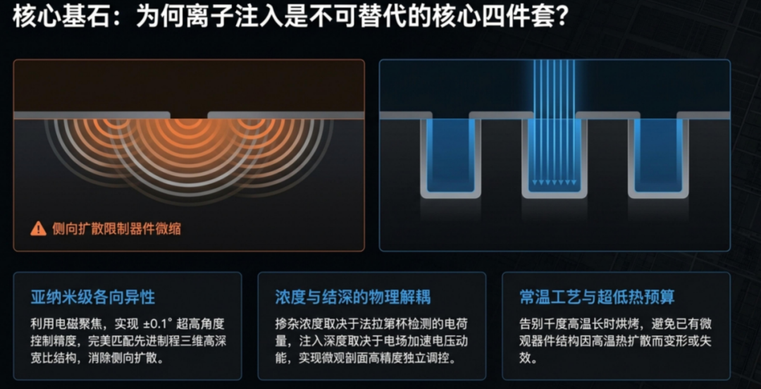
What Key Values Does Ion Implantation Hold Amid Continuous Process Shrinkage? Among the hundreds of process steps in IC (Integrated Circuit) manufacturing, doping is the core step that determines the electrical performance of semiconductor devices and constructs the microscopic PN junctions on the wafer. As one of the "Big Four" core tools in front-end semiconductor manufacturing, ion implanters, along with lithography scanners, etchers, and thin-film deposition equipment, form the technological cornerstone of modern wafer foundry lines. Its basic physical mechanism involves ionizing atoms of specific chemical elements (such as boron, phosphorus, and arsenic), accelerating them under a strong electric field to gain extremely high kinetic energy, and finally shooting them at high speed into the target silicon or compound semiconductor wafer. These high-energy ions gradually decelerate through collisions with substrate atoms and eventually stop at specific depths. Subsequent thermal annealing activation changes the conductivity type, resistivity, and mobility of local areas on the wafer. Compared with traditional chemical/physical thermal diffusion doping technologies, the ion implantation process demonstrates irreplaceable generational technological advantages in modern micro-nano manufacturing, completely overcoming the numerous physical limitations of thermal diffusion.
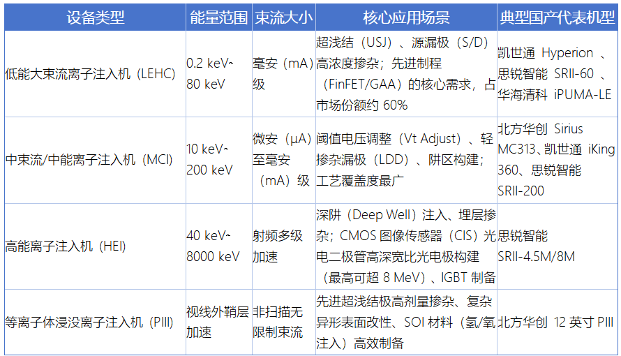
What Segmented Technology Lineage Has Ion Implantation Equipment Evolved Into Amid Diverse Doping Demands? To meet the diverse doping depth and concentration requirements in IC processes, ranging from Ultra-Shallow Junctions (USJ) to Deep Wells, ion implantation equipment has formed a highly segmented technology lineage through long-term industrial evolution.
What Are the Three Major Core Control Barriers for Ion Implanters? The technical barriers to R&D for ion implanters are extremely high, with complexity covering precision electromagnetics, high-vacuum technology, high-frequency microwaves, particle physics, and precision mechanical manufacturing. Its key core parameters and technical barriers are mainly reflected in the following three dimensions:
- Angle precision control: In sub-28nm and more advanced logic wafer manufacturing, the deviation of the projection angle at which the ion beam enters the wafer surface must be strictly controlled within ±0.1°. As line widths shrink, high-precision angle regulation can effectively avoid adverse interference from the channeling effect and shadowing effects on the electrical characteristics of the 3D channels on the wafer.
- Dose and uniformity control: The uniformity of the ion implantation dose directly determines the consistency of the threshold voltage of billions of transistors on the chip. The system needs to use advanced Faraday Cup arrays to dynamically and real-time measure the scanned ion beam, and feedback-regulate the scanning speed of the beam and the movement trajectory of the wafer stage, ensuring high-precision control of dose deviation and uniformity across the wafer surface.
- Energy purity and energy control: The energy deviation of ions is directly related to the precision of the implantation depth, requiring a system energy control precision of up to ±1%. High-energy ion implanters need to utilize high-frequency RF acceleration systems. Through precise phase joint debugging of dozens of resonant cavities, the ion energy is increased to the megaelectron-volt (MeV) level within a beamline of several meters, which involves extremely tedious joint debugging parameter control.
Although some equipment such as high-current implanters has been localized, the most fundamental core components of implanters, such as high-voltage power supply modules, high-precision mass analyzers (used to magnetically select a single ion beam with a specific mass-to-charge ratio), and ion source filaments, still highly rely on imports. These represent the deep-water zone that urgently needs to be conquered in the process of supply chain localization.
What Is the Unique Mechanism of PIII Plasma Immersion Ion Implantation? Compared with traditional beamline ion implanters, Plasma Immersion Ion Implantation (PIII) is a disruptive non-line-of-sight doping technology. Its working principle is to directly place the workpiece to be processed in a high-density plasma source and apply a high-voltage negative pulse bias to the workpiece. At this time, positive ions in the plasma will be accelerated by the electric field of the plasma sheath formed around the workpiece, shooting towards the workpiece surface from all directions in a comprehensive and isotropic manner.
Advantages: It completely breaks free from the "row-by-row and column-by-column" physical scanning limitations of traditional beamline implanters, enabling whole-wafer, high-efficiency implantation. In large-area processing and mass production (such as hydrogen/oxygen implantation for preparing SOI materials), efficiency can be increased by up to 10 times, with greatly simplified equipment design and significantly reduced process and fab construction costs. Diverse surface engineering applications: Beyond semiconductor manufacturing, PIII technology is also widely used in materials physics and biomedical fields. For example, in the field of biomedical materials such as titanium-based bone implants, using PIII technology to implant cobalt, silver, or zinc elements into the titanium-based surface can reduce the adhesion of tested bacteria (such as methicillin-resistant Staphylococcus aureus) by more than 80%. While promoting osteoblast adhesion, differentiation, and bone healing, it can block the risk of postoperative infection without antibiotics. In addition, PIII can also significantly improve the high-temperature oxidation resistance, wear resistance, and corrosion resistance of aero-engine blades and titanium/aluminum alloy components. Technical limitations: Plasma implantation itself also has certain technical bottlenecks. Because it relies on plasma sheath acceleration, it easily leads to non-uniformity of the implantation dose, and the depth of the implanted layer is usually relatively thin. In addition, under high-voltage operation, the system is extremely prone to instantaneous arcing. Therefore, pulse bias operation is usually required to prevent arcing and leave time for the plasma to recover its density around the workpiece. Interface physical mechanism: When using PIII for high-dose implantation, an ion-beam mixing effect is often formed. The intense collisions make the interface atomic structure chaotic and disordered, which can significantly improve the bonding force between the film and the substrate (which can be verified by scratch tests). If the implantation dose exceeds the solid solubility limit of the implanted material, a brand-new nanoscale stable or metastable phase can be precipitated on the substrate surface through Ion Beam Synthesis, thereby comprehensively improving the mechanical and physical properties of the material.
Under the Global Duopoly Monopoly, What Is the Breakthrough Path for Domestic Ion Implantation Equipment Companies? The global semiconductor ion implantation equipment market exhibits the characteristics of a highly concentrated duopoly. According to multi-dimensional statistics from third-party market research institutions, this market has shown a steady growth trend in recent years.
In terms of regional distribution, the Asia-Pacific region, led by China, Japan, and South Korea, is the absolute core driving force for global semiconductor ion implantation equipment. In 2025, the Asia-Pacific region accounted for the largest global market share with approximately 30.56%, followed by North America (accounting for about 25%27%) and Europe (accounting for about 20%22%).
From the perspective of global supply-side competition, Applied Materials and Axcelis jointly monopolize about 90% of the global market share (Gartner): Applied Materials: Relying on the classic acquisition of Varian, it has long held a dominant position in the ion implantation field, with an overall market share of over 50% (as high as 70% within select mature-node manufacturing segments). Its product line comprehensively covers high-current, medium-current, and ultra-high-dose ion implantation. Since 2000, AMAT's market share has long been stable at over 30%, and even reached an absolute dominant level in some years. Axcelis: It mainly has absolute dominance in the high-energy ion implanter track, its share in the high-energy ion implanter segment reaches 55%. In 2020, its revenue was 475 million US dollars, and its net profit was 50 million US dollars. Nissin: With medium-current ion implanters as its main product, its market share is about 10%. Nissin has successfully won bids and achieved batch delivery of ion implanters in domestic projects such as the Gu'an OLED project and the Hefei Jinghe 12-inch mass production line.
Faced with long-term market blockades and technological monopolies by overseas giants, domestic Chinese ion implantation equipment manufacturers, driven by national policies, capital intervention, and the strong supply chain security demands of wafer fabs, have embarked on a process of accelerated catch-up.
Kingsemi Covers high-current for advanced logic, high-current for advanced memory, and medium-current (supporting high-temperature/cryogenic); In 2025, Kingsemi posted revenue of RMB 348 million (USD ~47 million), representing a 44.55% year-on-year increase; in 2025, it delivered over 10 and accepted over 15 12-inch tools, with cumulative throughput breaking through 10 million wafers; in March 2026, it released the Hyperion high-current implanter for advanced processes and the new iKing 360 medium-current implanter. As a leading local supplier advancing supply chain independence, relying on its major shareholder Advanced Technology Group, it achieves vertical integration and synergy of the industrial chain of "semiconductor equipment + core components + new materials".
Xinyu Semiconductor (HWATSING) 12-inch low-energy high-current (iPUMA-LE) and low-temperature implanter for advanced processes (iPUMA-LT). At the end of 2024, HWATSING fully acquired Xinyu Semiconductor for no more than 1.005 billion RMB; in July 2025, the first 12-inch low-temperature implanter iPUMA-LT was delivered to a domestic logic leader; from 2025 to 2026, the high-current iPUMA-LE will be delivered in batches to domestic leading logic/advanced memory wafer fabs. Relying on HWATSING's powerful CMP customer channels and brand effect, it achieves rapid market penetration of high-current and low-temperature key process equipment, accelerating the pace of scaled volume production.
SRI Semiconductor High-energy RF implanter (SRII-4.5M/8M, covering 28nm/max 8MeV) and high-current implanter (SRII-60/200). In 2023, the first high-energy ion implanter achieved a breakthrough and secured customer orders; in 2024, high-energy ion implanters accelerated domestic substitution in frontier mass production lines such as CIS. Technologically leading in the high-energy implantation field, it achieves RF band transmission efficiency of up to 30%~50% and energy resolution of up to ±1% (significantly better than the industry average of ±2.5%).
NAURA Medium-current silicon IC implanter (Sirius MC313), SiC high-temperature implanter, and 12-inch plasma immersion implanter; in March 2025, at the SEMICON China conference, the Sirius MC313 12-inch implanter was officially released, marking its official entry into the ion implantation equipment market; simultaneously launching a dedicated high-temperature tool for SiC; as a platform-based semiconductor equipment giant, by incorporating ion implantation equipment into its vast front-end process portfolio (etching, thin-film, cleaning, etc.), it provides one-stop, comprehensive front-end doping and etching/electroplating solutions.
CETC Zhongkexin Electronics Equipment Full-spectrum coverage of medium/high-current and high-energy implanters; successfully achieved the localization of the full-spectrum products of ion implanters, possessing the capability to provide one-stop implantation solutions for global foundries, and continuing to scale up volume production in domestic fabs; as one of the earliest major entities to tackle implanters domestically, it has played a foundational and cornerstone substitution role in the mass production lines of high-current and medium-current for mature processes.
The structural opportunities in segmented tracks will be further broken down below: Mature Processes: High Integration, High Capacity, and CIS Special Process Opportunities Amid the rapid expansion of mature process capacity in mainland China, mature process ion implantation equipment still possesses a massive market base. The structural dividends in this track are mainly concentrated in the upgrading of logic process platforms and the volume production of specific devices (such as CMOS Image Sensors (CIS) and IGBT power devices).
For instance, the high-energy, high-MeV-level demand brought by CIS: As the requirements for smartphone camera pixels and automotive intelligent driving cameras increase, the photodiodes of CIS need to develop towards extremely high aspect ratios to improve photoelectric conversion efficiency and reduce noise. This requires ion implantation equipment to provide precise deep implantation with high energy (typically 8 MeV or even exceeding 10 MeV). Consequently, high-energy ion implanters have become indispensable and highly premium tools in CIS mass production lines.
Domestic companies such as SRI Semiconductor with its SRII-8M are targeting this high-energy segmented track, achieving a breakthrough in this special mature process by adopting an advanced RF acceleration system.
Advanced Processes: Key Process Nodes of Shallow Junctions, Cryogenic Implantation, and Plasma Immersion When wafer process nodes shrink below 28nm and further evolve towards 14nm/7nm/5nm FinFET and GAA architectures, the ion implantation process faces unprecedented physical challenges: Source/drain Ultra-Shallow Junctions (USJ): Requires extremely low implantation energy (<1 keV) and extremely high implantation doses, which causes "beam divergence" in traditional beamline implanters due to the Space Charge Effect. In this scenario, developing high-dose, ultra-low-energy high-current implanters, or introducing 12-inch Plasma Immersion Ion Implantation (PIII) equipment, becomes a physical necessity. Cryogenic Implantation: During high-dose doping, collisions of high-energy ions will completely amorphize the single-crystal lattice of silicon on the wafer surface. To precisely control the depth of the amorphized layer and suppress Transient Enhanced Diffusion (TED) during subsequent annealing, the industry has introduced cryogenic/ultra-low-temperature (typically below -100°C) implantation processes.
High-Temperature Resistance Technical Requirements for Third-Generation Semiconductors (Represented by SiC and GaN) Driven by the high-efficiency conversion requirements of NEVs (New Energy Vehicles), photovoltaic energy storage, and AI server PMICs (Power Management ICs) (PSU (Power Supply Unit), VRM (Voltage Regulator Module), POL (Point-of-Load)), the application of third-generation semiconductor (wide bandgap semiconductor) materials is experiencing explosive growth.
Because the bandgap of silicon carbide (SiC) is about 3 times that of silicon, the breakdown electric field strength is about 10 times that of silicon, and the thermal conductivity is 3.3 times that of silicon, SiC devices can operate stably in extreme environments of high frequency, high voltage, high-temperature resistance, and ultra-low loss.
However, the carbon-silicon covalent bond energy in SiC is extremely high, and its lattice structure is extremely hard. Ion implantation at room temperature will cause severe damage to the SiC lattice and produce an amorphized layer on the surface that cannot be repaired by thermal annealing.
To overcome this physical limitation, SiC device manufacturing must adopt ion implantation systems with high-temperature control: High-temperature implantation: During the implantation process, the wafer is heated to ultra-high temperatures of 500°C or even 1000°C. High-temperature implantation can provide lattice atoms with sufficient dynamic thermal energy to perform "in-situ lattice self-repair" (Dynamic Annealing) at the moment of ion collision, thereby preventing complete amorphization of the lattice and greatly improving activation yield. Temperature uniformity barrier: This poses a harsh challenge to implanters. The equipment target chamber and Electrostatic Chuck (ESC) must achieve extremely superior temperature uniformity control under ultra-high temperature, high pressure, and high-current beam conditions.
Future Industry Trends and Domestic Breakthrough Paths Currently, the evolution trends of the global and Chinese ion implanter industry present the following situations:
- Platform integration and full coverage of product matrix: The R&D of a single ion implanter is time-consuming, requires high upfront investment, and faces towering customer verification barriers. Global giants like AMAT have achieved platform-based supply through M&A and multi-category equipment synergy. Domestic equipment companies are also evolving in this direction. Platform-based semiconductor equipment giants such as NAURA and HWATSING are gradually building "process toolkits" (such as HWATSING's "CMP + ion implantation" and NAURA's "etching + thin-film + cleaning + implantation + electroplating") through independent R&D or M&A holdings, reducing customer entry barriers through synergy effects.
- Supply chain localization and underlying ecosystem security: Although high-current implanters have achieved domestic substitution in some fabs, the towering technical barriers of ion implanters are also reflected in the underlying core components—high-voltage power supply modules, high-precision mass analyzers, ion source filaments, and electrostatic chucks still highly rely on imports. The focus of future breakthroughs will inevitably extend to the deep-water zone of underlying components in the industrial chain. Improving the localization rate of the supply chain and establishing a local component supply alliance have become important topics for ensuring production security.
Facing the nearly monopolistic competitive landscape of international giants, for domestic manufacturers to increase their market share from the current extremely low level (industry estimates show that the combined market share of Chinese ion implanter suppliers remains below 5%) to over 15% in the next two to three years, they can break through via the following three paths: Path 1: Building an Integrated Ecosystem for the Entire Semiconductor Industry Chain The operating model of Kingsemi provides an excellent sample of industrial breakthrough. Relying on its major shareholder Advanced Technology Group, Kingsemi not only exerts efforts at the system assembly level but also actively coordinates with the group's advantages in basic materials (such as bismuth metal and other advanced functional materials) and independent R&D and supply of core components to jointly tackle underlying "choke point" problems such as high-precision mass analyzers, ensuring the autonomy and security of the supply chain.
This vertical integration strategy of "equipment and core component synergy" has greatly improved supply chain resilience and reduced dependence on overseas supply chains, making it expected that Kingsemi's shipment volume in 2026 will surge significantly, striving to break through the milestone of 60 units shipped annually.
Path 2: Single-Point Breakthrough in Segmented Tracks, Empowering Brands with Benchmark Customers New entrants should avoid full-scale melee with overseas giants, but instead choose the most urgent segmented process links with the lowest domestic production rate for precise tackling.
HWATSING (Xinyu Semiconductor): Concentrating advantageous resources to tackle advanced memory and cryogenic high-current, its low-energy high-current implanter iPUMA-LE and cryogenic high-current implanter iPUMA-LT have completed verification and obtained batch orders at memory leaders and logic giants respectively, breaking the ice of foreign giants at ultra-low temperature and key high-current nodes in one stroke, achieving single-point explosion of business and accelerating scaled application. Its parent company HWATSING adopts a gradual equity acquisition strategy, first taking a stake to incubate, and then fully acquiring it at the end of 2024 for no more than 1.005 billion RMB, avoiding the financial risks of early R&D and laying an excellent capital and industrial foundation for the comprehensive explosion of the ion implantation series. SRI Semiconductor: Relying on years of precipitation in high-energy RF acceleration technology, it specializes in MeV-level high-energy ion implanters, achieving deep binding and breakthroughs in the high-end mature track of CIS image sensors.
Path 3: Broadening the Product Platform Horizontally and Deepening One-Stop Delivery Vertically As the semiconductor industry enters a new round of capacity expansion cycle, fabs are more inclined to reduce supplier management costs and procure one-stop process toolkits. As a leader in domestic semiconductor equipment, NAURA high-profilely released its first Sirius MC313 12-inch medium-current ion implanter and plasma immersion equipment at the SEMICON China conference. Its core strategy is to incorporate ion implantation equipment into its already mature overall front-end process toolkit for wafer manufacturing, logic chips, and compound semiconductors.
In addition, on the same day as the release of the Sirius MC313, NAURA also heavily launched its first 12-inch TSV (Through-Silicon Via) copper filling electroplating equipment, Ausip T830. This strategy of organically bundling implanters with existing heat treatment, etching, cleaning, and electroplating equipment and conducting technical joint debugging can provide fabs with a complete set of doping and junction formation technical solutions, significantly shortening customers' whole-line process debugging time. This will also become the core driving method for domestic implantation equipment to achieve leapfrog market share improvement in the future.
Conclusion As the core barrier equipment in semiconductor chip manufacturing, the localization of ion implanters has moved from the simple "whole machine assembly" stage into the advanced process tackling period represented by "cryogenic, ultra-high energy, and plasma immersion," as well as the deep-water zone of underlying component localization represented by "high-voltage power supplies, high-precision mass analyzers, and high-temperature electrostatic chucks."
References:
- Progress in antibacterial/osteogenesis dual-functional surface modification strategy of titanium-based implants - PMC, https://pmc.ncbi.nlm.nih.gov/articles/PMC10581867/
- Research Progress on Wide Bandgap Silicon Carbide Wafer Bonding - Researching, https://www.researching.cn/ArticlePdf/m00001/2025/52/18/1803008.pdf