
By Peng Cheng On April 20, 2026, Wetzlar in Germany and Changchun in China, two cities separated by thousands of miles, completed a two-way journey that is set to rewrite the landscape of the global imaging industry. Leica, an international top-tier optical brand, and Gpixel (Changguang Chenxin), a domestic high-performance CMOS manufacturer, officially announced a strategic partnership. The two parties will jointly customize and develop high-performance CMOS image sensors for the next generation of Leica cameras.
It must be understood that over the past few decades, almost all mainstream camera brands, including Leica, Hasselblad, Nikon, Panasonic, and Ricoh, have deeply relied on Sony for the core CMOS of their high-end models. Canon has formed a closed loop with its fully self-developed technology, and Japanese manufacturers have firmly built an iron curtain for high-end image sensors. Domestic CIS, on the other hand, has long been confined to the fierce competition within the small-size track of 1-inch and below for smartphones, and has barely held any market presence in the large-format field of professional cameras.
This time, Gpixel brought China's self-developed large-format CMOS to enter the supply chain of the world’s top imaging brands. This is not a simple supply chain cooperation, but a genuine industry turnaround for domestic CIS. Chinese CIS chips have finally opened a breach in the high-end camera market.
01. Monopoly and Absence: The Global CIS Landscape and the "Scale vs High-End" Dilemma of Domestic Brands
In the world of digital imaging, there is an unspoken industry iron rule—"a larger sensor beats a smaller one." What determines the upper limit of a camera's image quality is always that CMOS image sensor. And this core chip, which can be called the "heart of the camera," has been almost completely held in the hands of Japanese manufacturers over the past two decades.
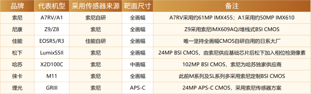
In the global interchangeable lens camera market, the sensor supply chain presents a highly concentrated market structure. Sony itself is both a camera manufacturer and the world's largest image sensor supplier, with its semiconductor division long supplying CIS chips to external brands. Relying on its vertical integration capabilities, Canon has insisted on self-developing and self-producing CMOS since the DSLR era, forming a closed loop from wafers to complete machines. Apart from this, almost all Japanese and German high-end camera brands are deeply dependent on Sony's sensor supply.
Although Nikon historically used chips from suppliers such as Toshiba and Aptina, after entering the full-frame mirrorless era, the core sensors of its Z-series models basically come from Sony. The sensor supply chains for Panasonic's L-mount full-frame models and Fujifilm's medium-format GFX series are also closely tied to Sony. In more niche high-end fields, Hasselblad's medium-format systems, Ricoh's GR series, and even many previous Leica models have all been equipped with Sony IMX series sensors.
Leica's sensor route is particularly dramatic. This century-old brand, known for its "German flavor" optics, cooperated with the Belgian company CMOSIS in the early days of digitalization to customize sensors for the M240. After Leica teamed up with CMOSIS for the second time to launch the M10 in 2017, several founding members and key figures of CMOSIS left the company in 2018 and joined Gpixel. Today, Leica has once again chosen Gpixel to customize chips for it. History seems to have drawn a circle, only the center has moved from Antwerp, Belgium, to Changchun, China. Before the cooperation between Leica and Gpixel, no Chinese enterprise's CIS chip had truly entered the core imaging chain of international high-end camera brands.
02. Domestic CIS: From Small Format to Large Format
The reason why a solid monopoly pattern has formed in large-format CIS for high-end cameras lies in its extremely high technical threshold. Compared to the small-size CIS of 1-inch and below commonly used in smartphones, the full-frame and above large-format chips required by professional cameras not only need to achieve ultra-high pixel integration but also need to achieve an ultimate balance in pixel architecture design, signal-to-noise ratio control, dynamic range, color reproduction accuracy, low-light imaging performance, and high-speed readout capabilities. Meanwhile, large-format chips have far higher requirements for wafer manufacturing processes, stitching technology, and mass production yield rates than ordinary consumer-grade chips.
This has also led to domestic CIS failing to enter the high-end professional imaging field for a long time. However, domestic CIS is not without development achievements; rather, it has long fallen into the development dilemma of "advantage in scale, lag in high-end," namely "half the sky in scale, not an inch of progress in high-end."
In the consumer mid-to-low-end market, domestic manufacturers have achieved scale breakthroughs. In the smartphone track of 1-inch and below small-size CIS, companies such as GalaxyCore, SmartSens, and OmniVision have continued to exert efforts, not only achieving large-scale mass production but also completing the domestic substitution of overseas brands in the mid-to-low-end market. In fields such as security surveillance and automotive imaging, domestic CIS occupies more than half of the global market share relying on its high cost-performance ratio and rapid customization advantages, among which OmniVision steadily ranks first globally in automotive CIS with a market share of over 30%.
These achievements are certainly gratifying, but essentially, they are still scale competition in the "small format" field. In the large-format field of professional cameras, domestic CIS has long been in a state of market blank. Although the industry has continuously heard news of technological breakthroughs, in 2021, the major special project "8K Ultra-HD Image Sensing Chip and System R&D" of "Core Electronic Devices, High-end General Purpose Chips, and Basic Software Products" (Core High-Base Program) led by Gpixel passed acceptance, launching the GCINE4349. This is the first domestic full-frame 8K stacked back-illuminated sensor, featuring 49 megapixels, 4.3μm pixels, 120fps in 8K mode, 240fps in 4K binning mode, a maximum dynamic range of 110dB (18+ stops), and a peak sensitivity of 75%. It supports professional formats such as 8K DCI and widescreen, facing film production, drones, and high-end cinematography, filling the gap in domestic 8K full-frame professional CIS.
This is the first time domestic sensors have adopted stacked technology on large-format chips, breaking Sony's technological monopoly in this field. In 2024, SmartSens and Nexchip joined forces to successfully trial-produce a 180-megapixel full-frame CIS based on the 55nm process platform and lithography stitching technology. This technology breaks through the limit size of a single mask through multiple exposure stitching, making it theoretically feasible for domestic sensors to have ultra-high pixels in the full-frame field.
However, such technological achievements have never been commercialized and have not been included in the supply chain system of any mainstream camera brand, falling into the dilemma of "technological breakthroughs but no market applications." Although Gpixel's GCINE4349 has entered the market with DJI's high-end imaging platform, it mainly targets professional cinema cameras and industrial fields, rather than traditional interchangeable lens cameras. It was not until the official announcement of the cooperation with Leica that domestic large-format CIS truly obtained commercial endorsement from a world-top imaging brand.
03. Accumulation and Breakout: From Scientific Research and Industrial Grade to Civilian High-End Imaging
Against the backdrop where the industry generally believes that the commercial landing of domestic large-format CIS still needs time, the cooperation between Gpixel and Leica has pushed the breakthrough of domestic imaging chips into a new stage. This cooperation is not accidental but the inevitable result of Gpixel's more than ten years of technological accumulation, and it is also the first time domestic high-end CIS has passed the comprehensive certification of global top-tier imaging standards.
Gpixel has relatively low visibility in the consumer market, but in the field of high-end industrial and scientific-grade CIS, the enterprise has become a global top player. Founded in 2012, relying on the profound scientific research accumulation of the Changchun Institute of Optics, Fine Mechanics and Physics, Chinese Academy of Sciences, Gpixel has deeply engaged in the R&D and design of high-performance CIS for more than ten years and is a top-three global designer of high-end industrial/scientific-grade CIS. Since its establishment, the enterprise has avoided the red ocean competition of small-size CIS for mobile phones, focusing on the higher technical threshold industrial and scientific-grade high-end track, and gradually breaking through core technological bottlenecks.
In 2014, Gpixel developed the world's highest resolution 150-megapixel CIS at that time; In 2015, it launched the world's first back-illuminated scientific-grade CIS; In 2021, it released the market's highest resolution 152-megapixel global shutter CIS at that time; In 2024, it launched an ultra-large format CIS with 100 megapixels and a photosensitive area of 65.5mm×65.5mm, widely used in high-end scenarios such as aerial surveying and astronomical observation. Over more than ten years of development, Gpixel has accumulated independent core technologies in key fields such as global shutter pixels, high-sensitivity pixels, low-noise circuits, high-speed readout circuits, and 3D wafer stacking, building a solid technological barrier.
The technological accumulation in the industrial high-end track has laid a solid foundation for Gpixel to enter the consumer professional imaging market. From the GMAX series industrial large-format chips to the industrialization of 8K ultra-HD image sensing chips, and then to the R&D of the GCINE series full-frame CIS for professional imaging, Gpixel has gradually completed the technological extension from industrial grade to consumer grade. It has not only broken through large-format CIS design technology but also established a mature mass production and quality control system, providing core support for the cooperation with Leica.
The cooperation between Gpixel and Leica is not a simple chip procurement and supply but deep collaboration covering the entire process of R&D and mass production, belonging to true joint customized development.
According to the cooperation details announced by both parties, the CIS customized exclusively for Leica's next-generation cameras will deeply integrate Leica's century-old technical experience in high-end imaging with Gpixel's leading sensor design capabilities, accurately matching Leica's stringent standards in color reproduction, noise optimization, dynamic range, and detail presentation. Notably, this cooperation integrates engineering and technical resources from three locations: Wetzlar, Germany (Leica headquarters), Antwerp, Belgium (Gpixel's European R&D center), and Changchun, China (Gpixel headquarters). Both parties will carry out full-process collaboration in chip verification, image tuning, mass production preparation, and other links, covering the complete industrial chain from chip design to complete machine landing.
04. What is Domestic Large-Format CIS Still Missing?
Domestic large-format CIS has made obvious progress in recent years, but compared with international giants such as Sony and Samsung in the high-end field, there are still systemic gaps.
Stacked process has not been completely broken through. High-end large-format CIS generally adopts a Back-Side Illumination (BSI) + stacked architecture, separating the pixel layer and the logic circuit layer to improve performance and integration. Domestic CIS lags behind the international advanced level in the stacked process, which is the key technological bottleneck for current domestic high-end CIS. SmartSens and Nexchip have signed a long-term deepening strategic cooperation agreement to go all out to tackle the domestic CIS stacked process.
Pixel performance and dynamic range. In application scenarios such as ultra-low illumination and high dynamic imaging, domestic sensors still face bottlenecks: the pixel quantum efficiency is low under low illumination, and the dark light sensitivity is difficult to meet high-end needs; the full well capacity of traditional pixel architecture is limited, and the single-frame dynamic range is insufficient. At present, the international advanced level has achieved a single-frame dynamic range exceeding 90dB, an area where domestic sensors still require further breakthroughs.
05. Supply Chain Puzzle: How Many Missing Pieces Remain for Domestic Camera Supply Chains?
Gpixel entering Leica is a single-point breakthrough in sensors. But if the perspective is elevated from "one chip" to "one complete machine," how complete is the supply chain of domestic cameras?
At the "mature" end, modules such as body structural parts, displays, batteries, and connectors, relying on the spillover effects from China’s consumer electronics and new-energy vehicle (NEV) industrial chains, already possess world-class manufacturing capabilities. The Huawei Pura 70 series has achieved a localization rate of over 90% except for the top configuration, proving that in the field of "non-precision optical machines," the Chinese supply chain boasts formidable integration capabilities.
In the "developing" middle segment, CIS and third-party lenses are breaking through rapidly. Brands such as Yongnuo, Viltrox, 7Artisans, and Meike have launched autofocus lenses covering full-frame and APS-C, with prices only one-third to one-half of those of Japanese original manufacturers. CFexpress cards leveraging YMTC’s Xtacking architecture have also been launched.
At the "high-risk, underdeveloped" end, core links such as Image Signal Processors (ISP), high-end body image stabilization, mechanical shutters, and ultrasonic motors still have low localization rates. Especially the ISP, which is the most fatal short board in the domestic camera supply chain. Canon's DIGIC X, Sony's BIONZ XR, and Nikon's EXPEED 7 are not only image processing chips but also the culmination of decades of color science, noise reduction algorithms, high-speed cache management, and AI subject recognition from each brand. Although domestic manufacturers have ISP accumulation in the fields of security and mobile phones, the requirements for real-time performance, power consumption, and algorithm collaboration in professional cameras are completely different.
What is worth looking forward to is that the breakthrough attempts of domestic cameras have never stopped. Liu Jingkang, CEO of Insta360, once publicly revealed that Insta360 is developing its own M43 mount camera; the magnetic imaging module previously released by Xiaomi also adopted an M43 specification sensor; including Songdian, multiple domestic brands have also successively spread the news of layout in the interchangeable lens camera market.