
By Feng Ning Recently, Shanghai Primarius Technologies Co., Ltd. (Primarius Technologies) announced that the acquisition of 100% equity in Chengdu Ruicheng Microelectronics Technology Co., Ltd. and 45.64% equity in Naneng Microelectronics (Chengdu) Co., Ltd. officially received the registration approval from the China Securities Regulatory Commission on June 26.
Following the transaction, Primarius Technologies will deeply integrate the IP resources of the two companies and establish a synergistic link between EDA and IP. However, beyond the finalization of capital, a more compelling question arises: when EDA and IP truly "merge," will the underlying rules of chip design be rewritten?
01. EDA + IP: Becoming the New Trend In chip design, EDA + IP can be described as a golden partnership. Here, IP refers to standardized design modules that have been tape-out verified and are reusable. Analogous to building with blocks, IP is equivalent to pre-formed block units that designers can directly invoke, significantly shortening the R&D cycle and lowering the design threshold. However, IP modules rely on EDA tools for integration and implementation. EDA is not only responsible for the layout, placement, and routing of various IPs and optimal interconnection, but also conducts multi-dimensional simulation and verification such as timing and power consumption, ensuring that performance indicators meet the standards under actual operating conditions of the chip.
Therefore, the "first pole" of the value embodied by EDA + IP is "synergy." It is reported that TSMC (Taiwan Semiconductor Manufacturing Company) started cooperating with IP vendors very early on and established the TSMC Open Innovation Platform (OIP). This platform has created a horizontally open industrial ecosystem. In addition to integrating resources from various IP vendors, it also connects EDA tool suppliers, cloud partners, design service centers, and numerous participants across the upstream and downstream of the industry chain.
The "second pole" of the value embodied by EDA + IP is localization. Since 2018, the United States has launched multiple rounds of restrictions targeting EDA tools. These include: in 2019 and 2020, the U.S. successively added several leading Chinese semiconductor and technology companies to the Entity List, restricting their access to high-end EDA software.
In 2022, the U.S. Department of Commerce revised the Export Administration Regulations (EAR) and added a new export control classification number ECCN 3D006, specifically targeting EDA tools that can be used to design GAAFET (Gate-All-Around Field-Effect Transistor) structures. These tools are primarily used for 3nm and below chip design.
On May 29, 2025, the U.S. Department of Commerce’s Bureau of Industry and Security (BIS) released restrictions mandating the Big Three EDA vendors (Synopsys, Cadence, and Siemens) to halt certain chip design software supplies to China.
In the global EDA market, U.S. manufacturers hold a monopoly. According to data from TrendForce, by 2024, these three U.S. companies held global EDA market shares of 32%, 29%, and 13%, respectively, with a combined market share as high as 74%. As for the domestic EDA market, the Big Three EDA vendors hold over 80% of the market share in China.
This series of changes has prompted the industry to deeply realize that while relying on global division of labor, it must accelerate the construction of the domestic EDA toolchain and IP ecosystem.
The "third pole" of the value of EDA + IP is the "great assist" from Chiplet and AI. AI brings two direct demands to EDA. First, the design object has been upgraded from "chip" to "system." AI data center design has evolved into a large-scale system engineering project encompassing heterogeneous computing power, high-speed interconnects, power supply and cooling, and power networks. EDA tools urgently need to expand from single-chip design to packaging-level and even system-level collaborative optimization, achieving cross-dimensional system design capabilities. Second, the design paradigm has shifted from DTCO (Design Technology Co-Optimization) to STCO (System Technology Co-Optimization). This means that EDA no longer just focuses on the process and performance of a single chip, but must coordinate collaborative innovation across multiple dimensions such as computing power, interconnects, memory, and packaging at the system level.
Meanwhile, the comprehensive implementation of Chiplet and Advanced Packaging technologies has also forced EDA tools to expand from single-chip design to packaging-level collaborative optimization. At the same time, the Chiplet model has also fundamentally changed the role of IP. Traditional IP is a functional module embedded in a single chip, while IP in the Chiplet era—especially Die-to-Die interface IP—has become the "bridge" connecting different chiplets. Its electrical characteristics, protocol compatibility, and physical implementation solutions directly determine the success or failure of the entire system.
02. Among the Big Three EDA vendors, Only Two Have Completed the Full EDA + IP Layout Synopsys: Proactively "Slimming Down" to Focus on EDA + foundational/Interface IP Synopsys is the player with the largest IP business volume among the Big Three EDA vendors. Financial report data shows that its IP business revenue in fiscal year 2025 was $1.75 billion. However, in early 2026, Synopsys made an unexpected decision—selling its processor IP solutions business to GlobalFoundries.
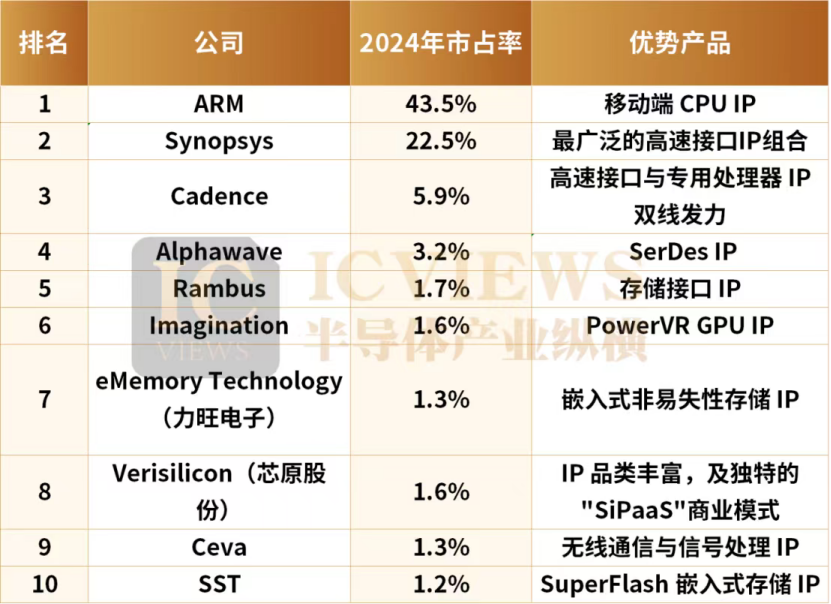
In January 2026, Synopsys announced that it had reached a final agreement to sell its processor IP solutions business to GlobalFoundries. This business includes ARC-V (RISC-V) and ARC CPU IP, DSP IP, NPU IP, and related software development tools.
Over the past decade, ARC, along with Arm and Tensilica under Cadence, has formed a tripartite structure, supporting the basic landscape of the global processor IP market.
Despite its strong technical strength, ARC faces increasingly fierce challenges in market competition. Over the past decade, the landscape of the processor IP market has undergone significant changes. The ARM ecosystem has grown increasingly powerful, the RISC-V open-source architecture has risen rapidly, and Tensilica under Cadence has achieved a reversal through continuous iteration, while ARC's market share has been declining. At that time, Synopsys chose to exit the increasingly competitive processor IP field and concentrate resources to consolidate its leading position in interface IP and foundational IP. Meanwhile, in July 2025, Synopsys completed its $35 billion acquisition of Ansys, integrating multi-physics simulation capabilities into the EDA stack.
It can be said that Synopsys's logic is to focus its firepower on the deep synergy between EDA tools and foundational/interface IP, trading a smaller range of IP categories for tighter EDA tool integration.
Cadence: Completing the IP Puzzle Through M&A Cadence's strategy in the IP track is completely opposite to that of Synopsys—it is aggressively acquiring assets.
In 2025 alone, Cadence announced the acquisition of Arm's Artisan foundational IP business and engineering team. This acquisition enabled Cadence to fill the gap in the foundational IP field and expand its design IP product line into the physical IP market. In September of the same year, Cadence also acquired the design and engineering business of Sweden's Hexagon AB for 2.7 billion euros, incorporating structural simulation, multi-body dynamics simulation, and other capabilities into its portfolio.
Today, Cadence is continuing to focus its growth priorities for the next five years on the three lines of EDA, IP, and SDA (System Design Analysis). Cadence CEO Anirudh Devgan stated, "The value of EDA and IP has significantly increased in 2026."
Cadence's logic is to trade capital for time, completing the IP capability matrix at once through large-scale M&A, and thereby challenging Synopsys's leading position in the IP track.
Siemens EDA: Partnering with OEMs to Leap Beyond In-House Development Mentor Graphics, the predecessor of Siemens EDA, also ventured into the IP field during its mid-development stage. A rich IP database can create synergistic effects for EDA tools, but it has not completed the "full suite of EDA tools + IP licensing" model. Currently, Siemens retains general foundational IPs such as USB, CAN, basic Ethernet, and standard memory compilers, while lacking high-performance CPU core IP and advanced high-speed PHY hard IP. Its means of making up for this is mainly through cooperation with OEM manufacturers. For example, in February 2025, Siemens announced that it had signed an exclusive OEM agreement for its EDA business to bring Alphawave Semi's high-speed interconnect silicon IP product portfolio to market through its sales channels.
It is introduced that this agreement includes Alphawave Semi's industry-leading IP platform for connectivity and memory protocols, such as Ethernet, PCIe, CXL, HBM, and UCIe (Die-to-Die) implementations. In addition to the IP sales channel agreement, the two companies will also collaborate to provide comprehensive Spec to Silicon Solutions by jointly engaging with customers and leveraging their respective capabilities and advantages.
03. Domestic EDA/IP Companies Have Two Paths to Take Currently, the development of domestic EDA tools and chip IP industries is relatively fragmented. Most enterprises focus only on a single track, and few manufacturers possess both a complete full-process EDA product line and a scaled independent IP matrix.
As for the reasons for the relative separation of EDA and IP: from the perspective of the sequence of industrial and technological development, IP emerged after EDA. The early emergence of EDA liberated the tediousness of manual design. The connection of multiple automated design software environments gradually formed the initial form of various design processes. Given the growth of design efficiency and the evolution of Moore's Law, the complexity of SoC (System on Chip) increased, and the demand for reusing standardized functional modules gave birth to the independent IP industry.
Then why haven't domestic EDA companies and domestic IP companies integrated very closely, or even consolidated into a single company?
Shen Li, CEO of Ruicheng Microelectronics, stated that first, due to the evolution of the division of labor in the industry chain across the entire industry, emerging IP companies can exist independently without necessarily having their own EDA tools. "In the current mature toolchain environment, these independent IP companies can choose customer-specified or industry-mainstream environments to deliver various IPs such as digital and analog IPs in the form of corresponding files."
Many Chinese semiconductor EDA and IP enterprises are still in the early stages of growth. Facing powerful overseas competitors, these companies often need to invest larger amounts of capital and resources to focus on developing their respective fields, making it difficult to change the relatively independent relationship in a short time. Furthermore, in terms of business operations, there are certain differences in the business models between EDA and IP companies. EDA companies usually provide broader solutions, including multiple links such as digital design, verification, placement and routing, simulation, and layout, while IP companies mainly provide design modules in chip design.
However, the industry landscape is now undergoing an obvious shift, and the integrated "EDA + IP" model is increasingly becoming the mainstream development direction of the industry. Domestic enterprises' layout in the integrated track is mainly divided into two development paths:
First, EDA enterprises rapidly expand their own IP product matrix through M&A of IP manufacturers. As mentioned at the beginning of the article, Primarius Technologies is rapidly complementing its own strength through this model. The acquired party, Ruicheng Microelectronics, covers products such as analog and mixed-signal IP, embedded memory IP, wireless RF communication IP, and wired connection interface IP; Naneng Microelectronics mainly deals in high-speed interface IP, analog and mixed-signal IP, etc.
Empyrean, a leading domestic foundational IP core supplier, relies on self-developed foundational IP while rapidly acquiring key IP technologies via M&A integration. In April this year, Empyrean announced that it plans to acquire 100% equity in Xinda Technology (Xiamen) Co., Ltd. in cash, with a transaction consideration not exceeding 250 million RMB. Xinda Technology is engaged in the development of memory/IP characterization extraction tools. This tool supports the development of DRAM/NAND Flash products, and its core products have entered the verification stage of major domestic wafer fabs. Empyrean stated that this acquisition aims to make up for the company's technical shortcomings in the field of memory chip design automation and accelerate the construction of a full-process EDA platform. In addition, Empyrean continues to seek investment and M&A opportunities by establishing industrial funds and other means.
Second, IP manufacturers continuously deepen IP supporting tools and carry out deep technical synergy with domestic EDA enterprises.
For example, high-speed interface IP leader Starblink (Xingyao Hui) independently developed supporting tools such as DDR log diagnosis and IP data analysis, which are used for timing and signal integrity debugging of high-speed PHY and controller IP. Starblink also uses GalaxSim, a simulator product from Empyrean (Xinhua Zhang Semiconductor), for IP simulation verification, achieving a close combination of domestic IP and domestic simulator verification.
VeriSilicon's business model is "Silicon Platform as a Service" (SiPaaS). Relying on independent semiconductor IP, it provides customers with platform-based, comprehensive, and one-stop chip customization services and semiconductor IP licensing services. In terms of IP reserves, VeriSilicon has very strong strength, possessing six types of processor IPs including GPU, NPU, VPU, DSP, ISP, and display processors, as well as over 1,600 mixed-signal IPs and RF IPs. VeriSilicon is also complementing its product line through M&A. In September last year, VeriSilicon disclosed an announcement that it plans to purchase a total of 97.007% equity in NICE Core Technology held by 31 transaction counterparties including Xinlai Gongchuang through issuing shares and paying cash, and raise matching funds.
It is reported that NICE Core Technology is one of the few suppliers focusing on RISC-V processor core IP and overall solutions. Its products cover alternatives to traditional ARM Cortex-M/R/C cores, etc. Its RISC-V IP has been mass-produced and adopted by more than 200 chip/system companies at home and abroad.
Looking ahead to the chip design industry in the next decade, a single EDA tool or an independent IP core cannot dominate the development context of the industry. The integrated fusion of EDA and IP is the key to determining the direction of the industry.